SG5768, SG5770, SG5772, SG5774
SG6506/SG6507/SG6508/SG6509
DESCRIPTION
The Linfinity series of diode arrays feature high breakdown, high speed
diodes in a variety of configurations.
Each array configuration consists of either common anode diodes,
common cathode diodes, or a combination of common anode and
common cathode diodes.
Individual diodes within the array have 60V minimum breakdown
voltage, can handle 500mA of current and typically switch in less than
10 nanoseconds.
Each of the array configurations is available in ceramic DIP or ceramic
flatpack and can be processed to JANTXV, JANTX, or JAN flows at
Linfinity's MIL-S-19500 facility.
DIODE ARRAY CIRCUITS
FEATURES
∑∑
∑∑
∑
60V minimum breakdown voltage
∑∑
∑∑
∑
500mA current capability per diode
∑∑
∑∑
∑
Fast switching speeds: typically less than
10ns
∑∑
∑∑
∑
Low leakage current
HIGH RELIABILITY FEATURES
MIL-S-19500/474 QPL - 1N5768
- 1N6506
- 1N5770
- 1N6507
- 1N5772
- 1N6508
- 1N5774
- 1N6509
JANTXV, JANTX & JAN available
LMI level "S" processing available
6/90 Rev 1.1 2/94
L
INFINITY
Microelectronics Inc.
Copyright
©
1994
11861 Western Avenue
Garden Grove, CA 92841
1
(714) 898-8121
FAX: (714) 893-2570
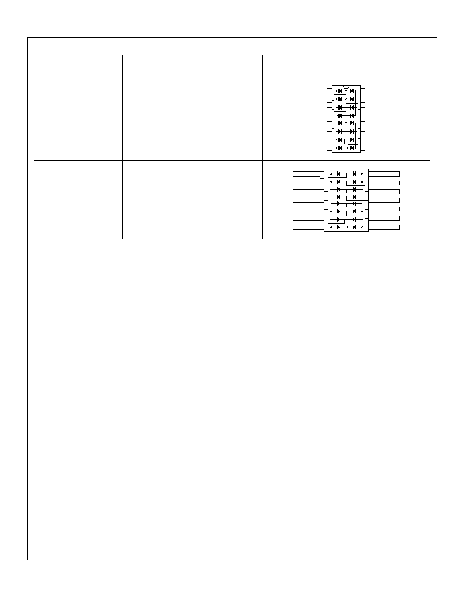
CIRCUIT DIAGRAMS
COMMON ANODE / COMMON CATHODE
SG5772/SG6508
DUAL COMMON ANODE / COMMON CATHODE
SG5774/SG6509
COMMON CATHODE
SG5768/SG6506
COMMON ANODE
SG5770/SG6507
DIODE ARRAY SERIES
6/90 Rev 1.1 2/94
L
INFINITY
Microelectronics Inc.
Copyright
©
1994
11861 Western Avenue
Garden Grove, CA 92841
2
(714) 898-8121
FAX: (714) 893-2570
ABSOLUTE MAXIMUM RATINGS
(Note 1 & 2)
Breakdown Voltage (V
BR
) ...................................................
Output Current (I
O
), T
C
= 25∞C
Continuous ................................................................
60V
500mA
Operating Junction Temperature
Hermetic (J, F Packages) ............................................
Storage Temperature Range ............................
150
∞
C
-65
∞
C to 200
∞
C
Note 1. Exceeding these ratings could cause damage to the device.
Note 2. Applicable for each diode.
J Package:
Thermal Resistance-
Junction to Case
,
JC
.................. 30∞C/W
Thermal Resistance-
Junction to Ambient
,
JA
.............. 80∞C/W
F Package (10 Pin):
Thermal Resistance-
Junction to Case
,
JC
.................. 80∞C/W
Thermal Resistance-
Junction to Ambient
,
JA
............ 145∞C/W
F Package (14 Pin):
Thermal Resistance-
Junction to Case
,
JC
.................. 80∞C/W
Thermal Resistance-
Junction to Ambient
,
JA
............ 140∞C/W
THERMAL DATA
Note A. Junction Temperature Calculation: T
J
= T
A
+ (P
D
x
JA
).
Note B. The above numbers for
JC
are maximums for the limiting
thermal resistance of the package in a standard mount-
ing configuration. The
JA
numbers are meant to be
guidelines for the thermal performance of the device/pc-
board system. All of the above assume no ambient
airflow.
Operating Ambient Temperature Range
SG5768 .......................................................... -55
∞
C to 150
∞
C
SG5770 .......................................................... -55
∞
C to 150
∞
C
SG5772 .......................................................... -55
∞
C to 150
∞
C
Operating Ambient Temperature Range
SG5774 .......................................................... -55
∞
C to 150
∞
C
SG6506 .......................................................... -55
∞
C to 150
∞
C
SG6507 .......................................................... -55
∞
C to 150
∞
C
SG6508 .......................................................... -55
∞
C to 150
∞
C
SG6509 .......................................................... -55
∞
C to 150
∞
C
RECOMMENDED OPERATING CONDITIONS
(Note 3)
Note 3. Range over which the device is functional.
ELECTRICAL CHARACTERISTICS
(Unless otherwise specified, these specifications apply for the operating temperature of T
A
= 25
∞
C for each diode. Low duty cycle pulse testing techniques
are used which maintains junction and case temperatures equal to the ambient temperature.)
1.0
1.1
1.5
1.0
100
50
4
40
20
V
V
V
V
V
nA
µ
A
pf
ns
Breakdown Voltage (V
BR
)
Forward Voltage (V
F
)
Reverse Current (I
R
)
Capacitance (C)
(Note 4)
Forward Recovery Time (t
fr
)
(Note 4)
Reverse Recovery Time (t
rr
)
(Note 4)
60
SG5768/SG6506
Test Conditions
Units
Parameter
Note 4. The parameters, although guaranteed, are not 100% tested in production.
Min. Typ. Max.
I
R
= 10
µ
A
Duty Cycle
2%, 300 µs pulse
I
F
= 100mA
I
F
= 200mA
I
F
= 500mA
I
F
= 10mA, T
A
= -55∞C
V
R
= 40V
V
R
= 40V, T
A
= 150∞C
V
R
= 0V, f = 1MHz, Pin-to-pin
I
F
= 500mA, t
r
15ns, V
fr
= 1.8V, R
S
= 50
I
F
= I
R
= 200mA, i
rr
= 20mA, R
L
= 100

DIODE ARRAY SERIES
6/90 Rev 1.1 2/94
L
INFINITY
Microelectronics Inc.
Copyright
©
1994
11861 Western Avenue
Garden Grove, CA 92841
4
(714) 898-8121
FAX: (714) 893-2570
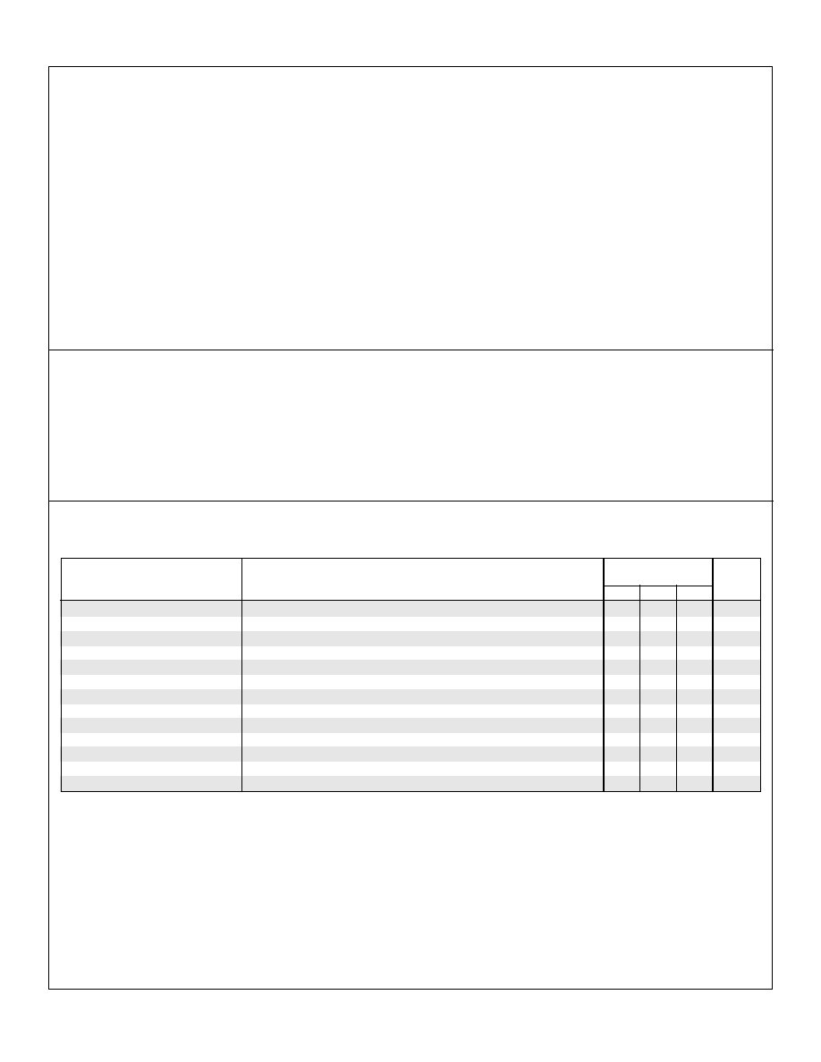
CONNECTION DIAGRAMS & ORDERING INFORMATION
(See Notes Below)
Ambient
Temperature Range
Part No.
Package
Connection Diagram
14-PIN CERAMIC DIP
J - PACKAGE
SG6506J
-55
∞
C to 150
∞
C
(1N6506)
-55
∞
C to 150
∞
C
SG5768F
-55
∞
C to 150
∞
C
(1N5768)
-55
∞
C to 150
∞
C
10-PIN CERAMIC FLATPACK
F - PACKAGE
SG6507J
-55
∞
C to 150
∞
C
(1N6507)
-55
∞
C to 150
∞
C
14-PIN CERAMIC DIP
J - PACKAGE
1
2
3
4
5
6
7
14
13
12
11
10
9
8
1
2
3
4
9
8
5
6
7
10
1
2
3
4
5
6
7
14
12
9
8
11
10
13
SG5770F
-55
∞
C to 150
∞
C
(1N5770)
-55
∞
C to 150
∞
C
SG6508J
-55
∞
C to 150
∞
C
(1N6508)
-55
∞
C to 150
∞
C
14-PIN CERAMIC DIP
J - PACKAGE
SG5772F
-55
∞
C to 150
∞
C
(1N5772)
-55
∞
C to 150
∞
C
1
2
3
4
5
6
7
8
10
9
1
2
3
4
9
8
5
6
7
10
1
7
6
5
4
3
2
14
13
8
9
10
11
12
10-PIN CERAMIC FLATPACK
F - PACKAGE
10-PIN CERAMIC FLATPACK
F - PACKAGE
Note 1. Consult factory for other packages available.
2. All packages are viewed from the top.
3. Consult factory for JAN, JAN TX, and JAN TXV product availability.